- 您现在的位置:买卖IC网 > Sheet目录486 > NTA4001NT1 (ON Semiconductor)MOSFET N-CH 20V 238MA SOT-416
�� �
�
�NTA4001N,� NVA4001N�
�Small� Signal� MOSFET�
�20� V,� 238� mA,� Single,� N� ?� Channel,� Gate�
�ESD� Protection,� SC� ?� 75�
�Features�
�?� Low� Gate� Charge� for� Fast� Switching�
�?� Small� 1.6� x� 1.6� mm� Footprint�
�?� ESD� Protected� Gate�
�?� AEC� ?� Q101� Qualified� and� PPAP� Capable� ?� NVA4001N�
�?� These� Devices� are� Pb� ?� Free� and� are� RoHS� Compliant�
�Applications�
�?� Power� Management� Load� Switch�
�?� Level� Shift�
�?� Portable� Applications� such� as� Cell� Phones,� Media� Players,�
�Digital� Cameras,� PDA’s,� Video� Games,� Hand� Held� Computers,� etc.�
�V� (BR)DSS�
�20� V�
�1�
�http://onsemi.com�
�R� DS(on)�
�Typ� @� V� GS�
�1.5� W� @� 4.5� V�
�2.2� W� @� 2.5� V�
�3�
�I� D� MAX�
�(Note� 1)�
�238� mA�
�2�
�MAXIMUM� RATINGS� (T� J� =� 25� °� C� unless� otherwise� stated)�
�N� ?� Channel�
�Parameter�
�Drain� ?� to� ?� Source� Voltage�
�Symbol�
�V� DSS�
�Value�
�20�
�Unit�
�V�
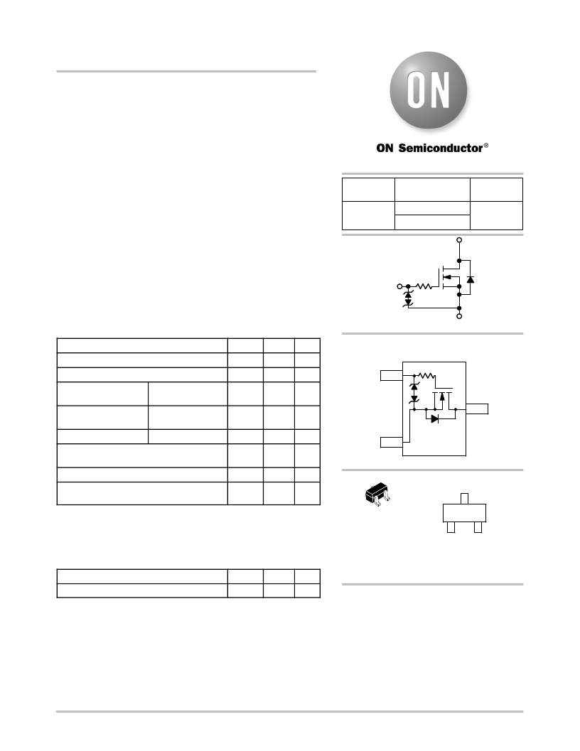
�PIN� CONNECTIONS�
�SC� ?� 75� (3� ?� Leads)�
�Gate� ?� to� ?� Source� Voltage�
�Continuous� Drain�
�Current� (Note� 1)�
�Steady� State� =� 25� °� C�
�V� GS�
�I� D�
�±� 10�
�238�
�V�
�mA�
�Gate�
�1�
�Power� Dissipation�
�(Note� 1)�
�Steady� State� =� 25� °� C�
�P� D�
�300�
�mW�
�3�
�Drain�
�Pulsed� Drain� Current� t� P� v� 10� m� s�
�Operating� Junction� and� Storage� Temperature�
�I� DM�
�T� J� ,�
�T� STG�
�714�
�?� 55� to�
�150�
�mA�
�°� C�
�Source�
�2�
�(Top� View)�
�Continuous� Source� Current� (Body� Diode)� I� SD� 238� mA�
�Lead� Temperature� for� Soldering� Purposes� T� L� 260� °� C�
�(1/8”� from� case� for� 10� s)�
�Stresses� exceeding� Maximum� Ratings� may� damage� the� device.� Maximum�
�Ratings� are� stress� ratings� only.� Functional� operation� above� the� Recommended�
�Operating� Conditions� is� not� implied.� Extended� exposure� to� stresses� above� the�
�Recommended� Operating� Conditions� may� affect� device� reliability.�
�3�
�2�
�1�
�SC� ?� 75� /� SOT� ?� 416�
�CASE� 463�
�STYLE� 5�
�MARKING� DIAGRAM�
�3�
�TF� M� G�
�G�
�1� 2�
�TF� =� Specific� Device� Code�
�THERMAL� RESISTANCE� RATINGS�
�Parameter�
�Junction� ?� to� ?� Ambient� –� Steady� State� (Note� 1)�
�Symbol�
�R� q� JA�
�Max�
�416�
�Unit�
�°� C/W�
�M� =� Date� Code�
�G� =� Pb� ?� Free� Package�
�(Note:� Microdot� may� be� in� either� location)�
�1.� Surface� ?� mounted� on� FR4� board� using� 1� in� sq.� pad� size� (Cu� area� =� 1.127� in� sq.�
�[1� oz]� including� traces).�
�ORDERING� INFORMATION�
�See� detailed� ordering� and� shipping� information� in� the� package�
�dimensions� section� on� page� 4� of� this� data� sheet.�
�?� Semiconductor� Components� Industries,� LLC,� 2011�
�October,� 2011� ?� Rev.� 2�
�1�
�Publication� Order� Number:�
�NTA4001N/D�
�发布紧急采购,3分钟左右您将得到回复。
相关PDF资料
NTA4151PT1
MOSFET P-CH 20V 760MA SOT-416
NTA4153NT1
MOSFET N-CH 20V 915MA SOT-416
NTA7002NT1
MOSFET N-CH 30V 154MA SOT-416
NTB13N10T4G
MOSFET N-CH 100V 13A D2PAK
NTB23N03RT4G
MOSFET PWR N-CHAN 25V 23A D2PAK
NTB25P06G
MOSFET P-CH 60V 27.5A D2PAK
NTB30N06T4
MOSFET N-CH 60V 27A D2PAK
NTB30N20T4G
MOSFET N-CH 200V 30A D2PAK
相关代理商/技术参数
NTA4001NT1G
功能描述:MOSFET 20V 238mA N-Channel RoHS:否 制造商:STMicroelectronics 晶体管极性:N-Channel 汲极/源极击穿电压:650 V 闸/源击穿电压:25 V 漏极连续电流:130 A 电阻汲极/源极 RDS(导通):0.014 Ohms 配置:Single 最大工作温度: 安装风格:Through Hole 封装 / 箱体:Max247 封装:Tube
NTA411
制造商: 功能描述: 制造商:undefined 功能描述:
NTA4141PT1G
制造商:ON Semiconductor 功能描述:
NTA4151P
制造商:ONSEMI 制造商全称:ON Semiconductor 功能描述:Small Signal MOSFET −20 V, −760 mA, Single P−Channel, Gate Zener, SC−75, SC−89
NTA4151PT1
功能描述:MOSFET -20V -760mA PChannel RoHS:否 制造商:STMicroelectronics 晶体管极性:N-Channel 汲极/源极击穿电压:650 V 闸/源击穿电压:25 V 漏极连续电流:130 A 电阻汲极/源极 RDS(导通):0.014 Ohms 配置:Single 最大工作温度: 安装风格:Through Hole 封装 / 箱体:Max247 封装:Tube
NTA4151PT1G
功能描述:MOSFET -20V -760mA PChannel RoHS:否 制造商:STMicroelectronics 晶体管极性:N-Channel 汲极/源极击穿电压:650 V 闸/源击穿电压:25 V 漏极连续电流:130 A 电阻汲极/源极 RDS(导通):0.014 Ohms 配置:Single 最大工作温度: 安装风格:Through Hole 封装 / 箱体:Max247 封装:Tube
NTA4151PT1G
制造商:ON Semiconductor 功能描述:P CHANNEL MOSFET -20V 760mA SC-75 制造商:ON Semiconductor 功能描述:P CHANNEL MOSFET, -20V, 760mA SC-75
NTA4151PT1H
制造商:ON Semiconductor 功能描述:PFET SC75 20V 760MA TR - Tape and Reel